- 您现在的位置:买卖IC网 > Sheet目录17367 > ADM1041-EVAL (Analog Devices Inc)BOARD EVALUATION ADM1041
ADM1041
AC_OK
This output is true when either AC SENSE 1 or AC SENSE 2 is true
+5V
(configurable). It can be configured as an open-drain N-channel
or P-channel MOSFET and as positive or negative (inverted)
logic. A pull-up or pull-down resistor is required. This pin can
be wire-ORed with the same pin on other ADM1041 ASICs in
the power supply. When the AC_OK pin is not used as such, it
1
V CC
MON2 10
MON3 16
can be configured as an analog input, MON5, or as a voltage
reference.
MON5
This is the alternative analog comparator function for the
7
MON5 18
–12V
THERMISTOR
AC_OK/V REF pin (Pin 18). The threshold is 2.5 V, and it has a
100 μA current source that allows hysteresis to be controlled by
adjusting the external source resistance. It is ideal for an OTP
sensing circuit using a thermistor as part of a voltage divider.
The OTP condition can be configured to latch off the power
supply (similar to OVP) or to allow an auto-restart (soft OTP).
OCP
2.5V
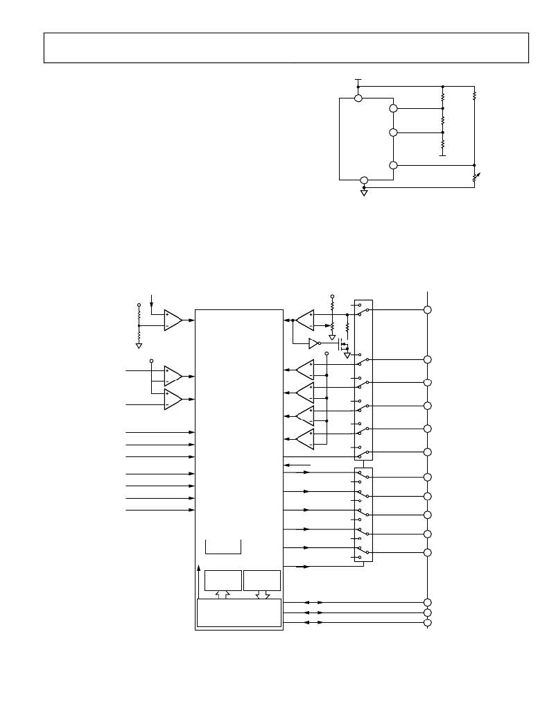
Figure 22. Example of MON Pin Configuration
In the preceding example, MON2 and MON3 are configured to
monitor a negative 12 V rail. MON2 is configured as negative
going OVP, and MON3 is configured as positive going UVP.
The 5 V power rail is used for bias voltage.
2.5V
18
OTP/
MON5
OCP
MON5
1.25V
OVP
1.5V
MON1
9
MON1
OVP
10 MON2
MON2
UVP
UVP
GENERAL
LOGIC
MON3
16 MON3
ACOK
ORFETOK
ACOK
ORFETOK
MON4
17 MON4
SHAREOK
SHAREOK
PSON
16 PSON
CLOCK
RESET
V DD OK
V DD OV
PENOK
RESET
V DD OK
V DD OV
PENOK
CONTROL
REGISTERS
PWRON
V REF
AC_OK
DC_OK
CBD
PEN
CONFIGURE
18 V REF
18 AC_OK
17 DC_OK
11 CBD/ALERT
12 PEN
I/Os
CONFIGURE
(WRITE
STATUS
(READ
REGISTERS) REGISTERS)
SDA/
CONTROL
PEN
14 PS ON LINK
LINES
SERIAL
INTERFACE
SCL
CS
13 SCL/
AC_OKLink
15 ADD0
Figure 23. Block Diagram of Protection and General Logic
Rev. A | Page 31 of 64
发布紧急采购,3分钟左右您将得到回复。
相关PDF资料
TDC225K025NSE-F
CAP TANT 2.2UF 25V 10% RADIAL
MIC59P50BWM
IC DRVR LATCH 8BIT PAR IN 24SOIC
A9AAT-0906F
FLEX CABLE - AFE09T/AF09/AFE09T
ISL85033EVAL2Z
EVAL BOARD2 FOR ISL85033
MIC5891BWM
IC DRVR LATCH 8BIT SER IN 16SOIC
MIC5891BN
IC DRVR LATCH 8BIT SER IN 16DIP
TAAB336K010G
CAP TANT 33UF 10V 10% AXIAL
SPX385AS-L-1-2
IC VREF SHUNT PREC 1.235V 8SOICN
相关代理商/技术参数
ADM10470J
制造商: 功能描述: 制造商:undefined 功能描述:
ADM1051
制造商:AD 制造商全称:Analog Devices 功能描述:Precision Dual Voltage Regulator Controllers
ADM1051A
制造商:AD 制造商全称:Analog Devices 功能描述:Precision Dual Voltage Regulator Controllers
ADM1051AJR
制造商:Analog Devices 功能描述:DC DC Cntrlr Dual-OUT Step Down 12V Input 8-Pin SOIC N 制造商:Analog Devices 功能描述:DC DC CNTRLR DUAL-OUT STEP DOWN 12V 8SOIC - Bulk 制造商:Rochester Electronics LLC 功能描述:ENHANCED DUAL BUS TERMINATOR - Bulk
ADM1051AJR-REEL
制造商:Analog Devices 功能描述:DC DC Cntrlr Dual-OUT Step Down 12V Input 8-Pin SOIC N T/R 制造商:Analog Devices 功能描述:DC DC CNTRLR DUAL-OUT STEP DOWN 12V 8SOIC N - Tape and Reel 制造商:Rochester Electronics LLC 功能描述:ENHANCED DUAL BUS TERMINATOR - Tape and Reel
ADM1051AJR-REEL7
制造商:Analog Devices 功能描述:DC DC Cntrlr Dual-OUT Step Down 12V Input 8-Pin SOIC N T/R 制造商:Analog Devices 功能描述:DC DC CNTRLR DUAL-OUT STEP DOWN 12V 8SOIC N - Tape and Reel 制造商:Rochester Electronics LLC 功能描述:ENHANCED DUAL BUS TERMINATOR - Tape and Reel
ADM1051AJRZ
制造商:Analog Devices 功能描述:DC DC CNTRLR DUAL-OUT STEP DOWN 12V 8SOIC N - Bulk
ADM1051AJRZ-REEL
制造商:Analog Devices 功能描述:DC DC CNTRLR DUAL-OUT STEP DOWN 12V 8SOIC N - Tape and Reel
